PCB Launch Optimization
Maximizing RF performance starts with a properly designed PCB launch. Amphenol RF understands the critical role that launch geometry plays in high-frequency and high-speed applications. That’s why we offer
collaborative support for PCB launch optimization, working closely with customers to ensure our connectors are seamlessly integrated into their unique PCB stack-ups and system designs.

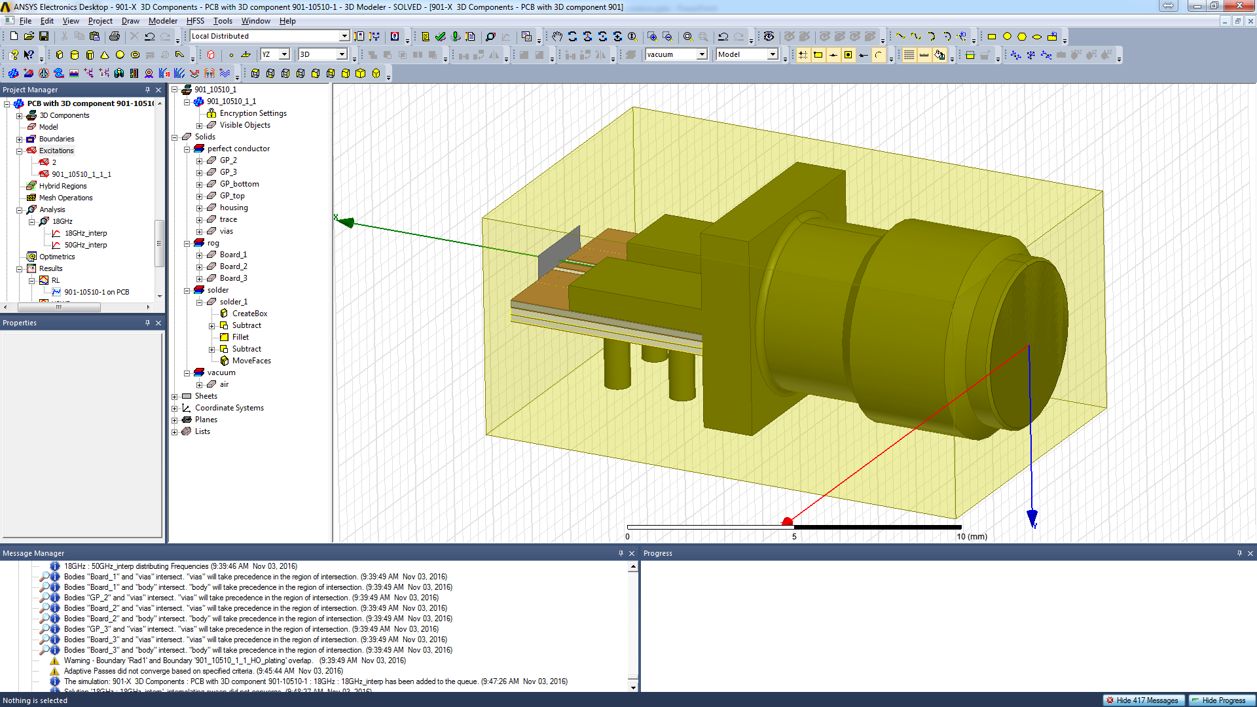
HFSS 3D Model
Collaborative Engineering Support
When working with Amphenol RF connectors, our team can:
-
Review your PCB stack-up and launch layout
-
Recommend optimized pad, anti-pad, and via geometries
-
Support performance validation using full-wave 3D simulation tools like ANSYS HFSS
-
Share technical guidance based on real-world application experience
This collaborative process can help reduce design iterations and accelerate time to market by ensuring reliable connector-to-board transitions early in the development cycle.
HFSS 3D Component Models
To further support design integration, Amphenol RF offers encrypted HFSS 3D component models for many of our board-mount connectors. These files allow engineers to simulate the performance of their system with Amphenol RF products included, improving confidence in signal integrity from the start.
Key Features:
Secure, encrypted models preserve IP while enabling accurate full-wave simulation
Easy integration into system-level HFSS projects (latest version of HFSS required)
Enables direct analysis of connector performance within your unique board layout
HFSS 3D component files can be found in the Product Resources section of applicable product pages.
Let’s Build It Right, Together
Amphenol RF is more than a connector supplier—we're your engineering partner. If you're designing with our connectors and want to ensure optimal launch performance, our technical team is ready to assist. From early concept through simulation and validation, we're here to support your success.
Explore available HFSS models on our product pages
Contact our Application Engineering team to discuss your design goals and how we can help optimize your PCB launch. An NRE charge may be necessary for more involved engineering efforts, for which our team will inform you prior to any work.

next design.
Send Us a Message
Please fill in the form below and we will contact you very soon.
Fields marked with an asterisk (*) are required.